
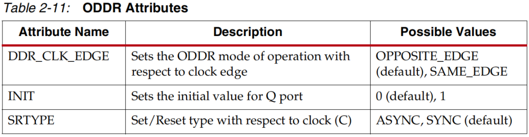
Certainly! Here is the translated text with the original HTML formatting intact:
In FPGA data transmission, the data sent by the FPGA is single-edge data, while the data sent by the PHY is double-edge data. Therefore, after sending a heartbeat packet, the FPGA must use the ODDR primitive to convert single-edge data into double-edge data. Typically, the FPGA processes data using the clock generated by the crystal oscillator (FPGA clock). Once the FPGA data is converted to double-edge data via the ODDR primitive, it synchronizes with the PHY clock. Thus, to transfer the data synchronized to the FPGA clock to the PHY chip, a cross-clock domain conversion is required, converting the FPGA clock-synchronized data into PHY clock-synchronized data. The conversion from single-edge to double-edge data is performed using the Output DDR primitive, or ODDR, which converts single-edge 8-bit data into double-edge 4-bit data.
Refer to the 7 Series FPGAs SelectIO Resources document and the Xilinx 7 Series FPGA Libraries Guide for HDL Designs for ODDR primitives.
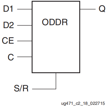
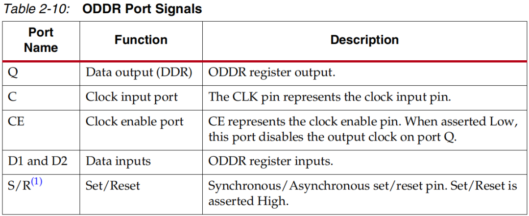
D1 and D2 are data inputs, CE is the ODDR enable, C is the clock, S and R are set and reset respectively, and Q is the output.
ODDR has two operating modes, configured as shown in the figure below: OPPOSITE_EDGE and SAME_EDGE.
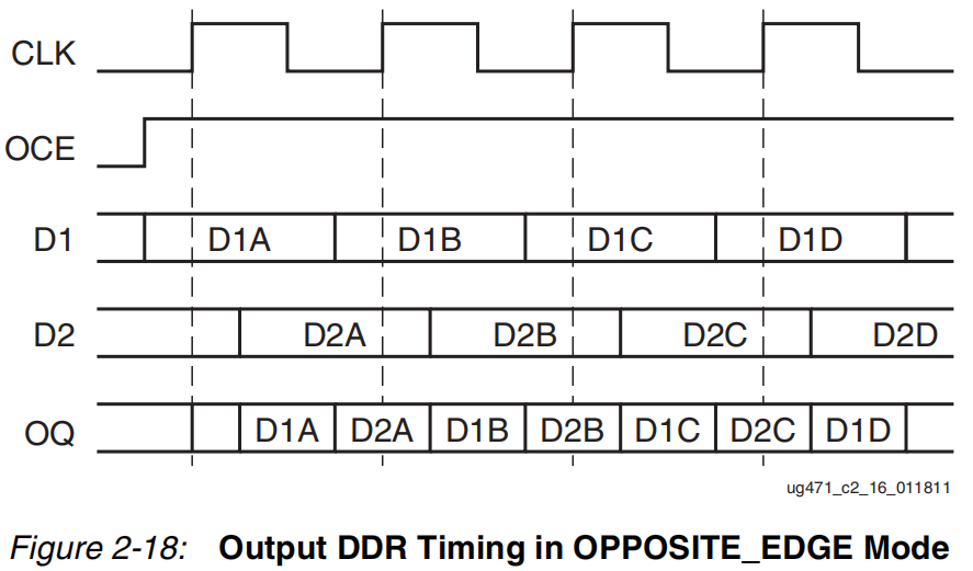
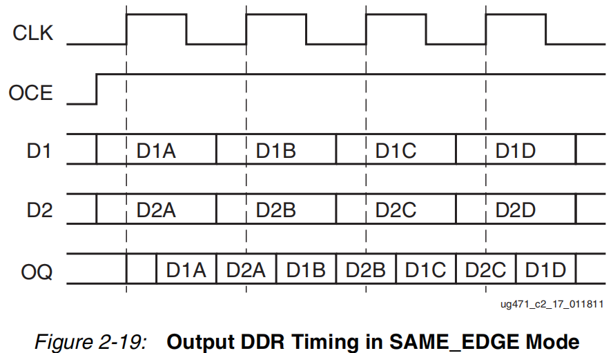
In OPPOSITE_EDGE mode, both edges are used to capture data, with the rising edge capturing low-order data D1 and the falling edge capturing high-order data D2. The output Q transmits D1 on the rising edge and D2 on the falling edge. In SAME_EDGE mode, only the rising edge is used to capture both low-order data D1 and high-order data D2, then D1 is transmitted on the falling edge of the output Q, and D2 is transmitted on the rising edge. In this transmission, we use the SAME_EDGE mode.
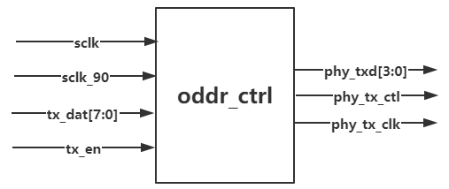
According to the hardware circuit diagram, the PHY transmits to the FPGA with one clock line, one enable line, and four data lines, all of which are double-edge data. The enable line contains DV and ERR, with the rising edge transmitting the DV signal (i.e., data valid signal) and the falling edge transmitting the ERR signal (i.e., data error signal, usually not considered as ERR is hardware-induced and unrelated to software). The four data lines contain a constant 8-bit data, with the rising edge transmitting bits 3:0 of the 8-bit data and the falling edge transmitting bits 7:4. We use the ODDR primitive to convert single-edge 8-bit data into double-edge 4-bit data, while extracting the 4-bit data corresponding to the valid DV signal. Thus, a module to achieve single-edge to double-edge functionality can be established: oddr_ctrl, with the input-output relationship diagram shown below. Finally, the phy_txd and phy_tx_ctl transmitted by the PHY chip are synchronized with the PHY clock phy_tx_clk. In the diagram, sclk_90 is the input clock signal formed by a 90-degree phase shift of the FPGA clock, aimed at making the conversion of phy_tx_rxd and phy_tx_ctl more stable. tx_dat and tx_en are the single-edge 8-bit data and corresponding data valid enable input to this module.
In the previous blog “Gigabit Ethernet (1)”, it was mentioned that the initialization of the PHY chip must meet the requirement, so do not forget the reset signal phy_rst_n of the PHY chip at the output port. This signal can be generated by a 4ms delay, and with this signal, the PHY chip can start working.
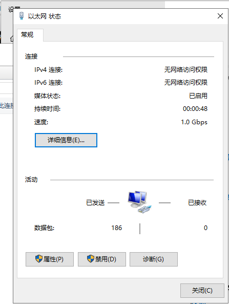
After mounting, open the Ethernet settings on the computer and change the adapter options to see the network card working normally.
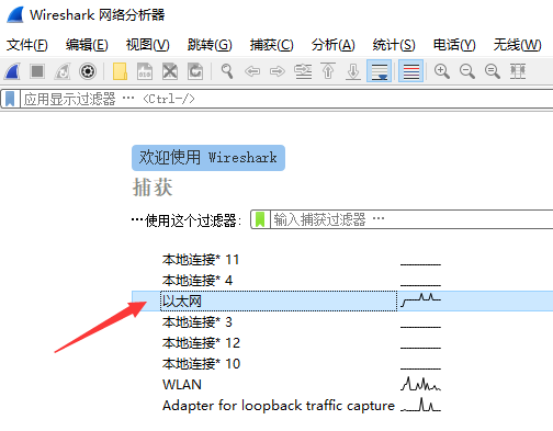
Open the Wireshark software, and you can see the waveform of the Ethernet changing.
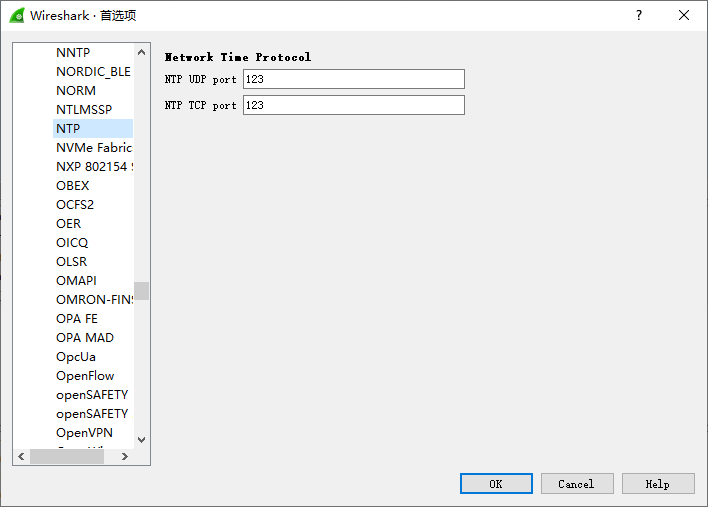
Double-click to enter, click Edit — Preferences, and click NTP to see our port number. This design uses UDP. Why look at NTP? Because NTP actually includes UDP and can be considered a type of UDP.
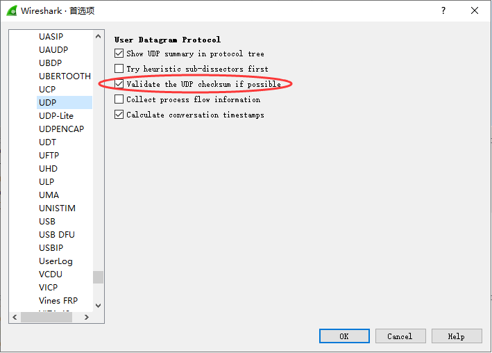
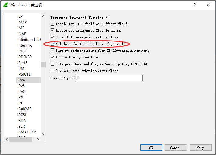
Click UDP and IPv4, check the UDP checksum and IP checksum, and you will see if the checksum is successful later.
Then we recapture the Ethernet, and you can see many blue parts indicating the heartbeat packets we transmitted. The black ones are not ours, as their Source and Destination are different from what we set, so we ignore them. Click on a blue stripe, and relevant information appears below. This information is after removing the packet header (7 55s, 1 d5), so the byte display is 106, which matches our design. Additionally, you can see the header checksum showing correct and Good, indicating that our checksum is also correct this time.
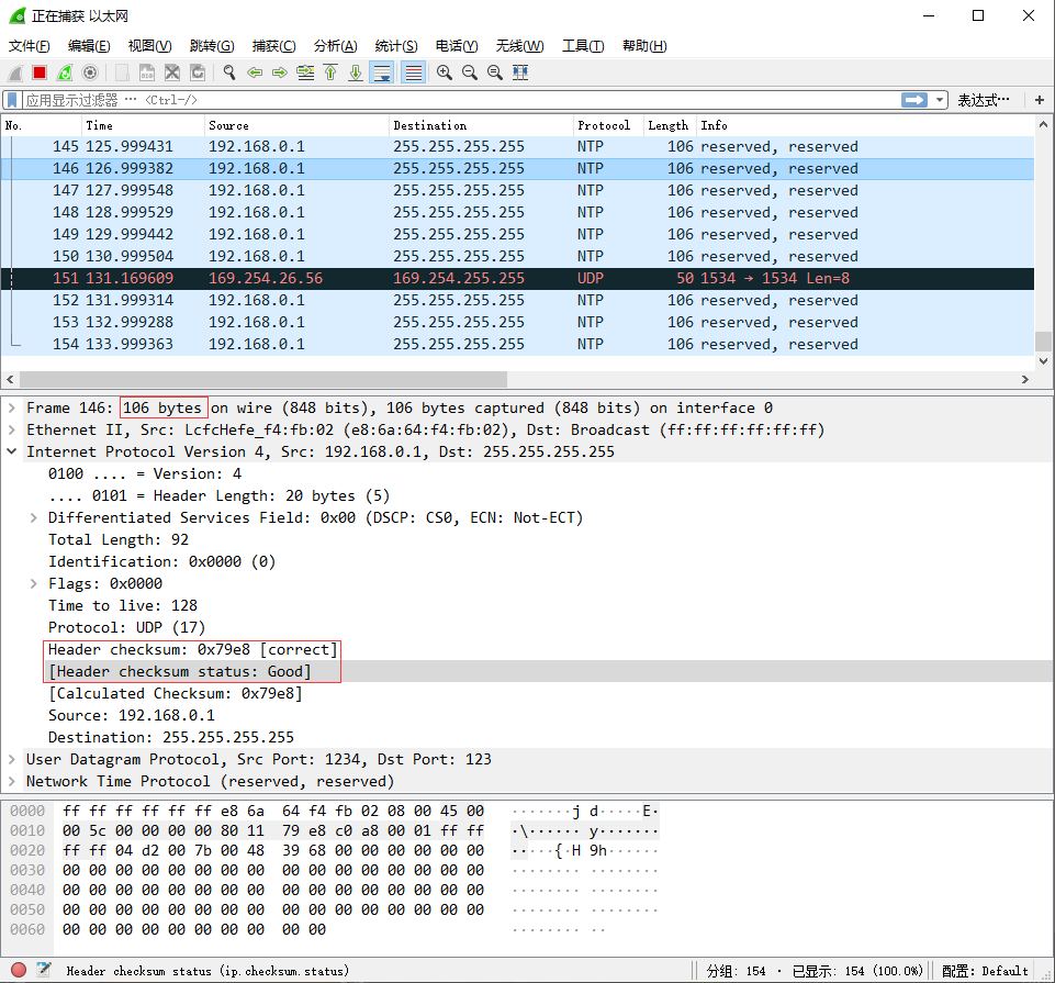
The above phenomenon indicates that our Gigabit Ethernet transmission project was successfully implemented. Mission accomplished!
“`I have translated the text while preserving the HTML structure and formatting. Let me know if you need further assistance!